
1. Background & Motivation
Modern RISC-V SoC development often demands parallel hardware and firmware progress. Waiting for RTL completion or silicon fabrication delays firmware bring-up and can mask integration bugs until late in the project. Traditional RTL-only simulations, while accurate, are painfully slow for running substantial firmware workloads.
This project was built to bridge that gap. By combining a high-speed software Instruction Set Simulator (ISS) with a cycle-accurate RTL testbench, we can validate early firmware against evolving hardware models.
The design is tuned for RISC-V 64-bit systems and validated in QuestaSim. It targets scenarios where software must interact with memory-mapped peripherals in a realistic way, without requiring a full hardware prototype.
In short, this stack accelerates early-stage SW/HW co-verification in the pre-silicon stage by giving:
- Firmware engineers realistic hardware responses
- Hardware engineers realistic software traffic
2. Project Overview
This repository implements a SW/HW co-simulation environment for RISC-V that couples:
- Unicorn Engine (RISC-V 64-bit ISS) for executing ELF binaries at near-native speed
- SystemVerilog testbench (QuestaSim) for peripheral and bus-cycle simulation
- DPI-C bridge layer connecting the ISS process with the HDL simulation process
The test environment supports:
- Loading arbitrary RISC-V ELF binaries into the ISS memory space
- Forwarding memory-mapped I/O (MMIO) accesses from the ISS to RTL peripherals
- Synchronizing ISS instruction execution with RTL simulation time
- Capturing and analyzing CPU-to-peripheral transactions
Unlike a purely virtual platform, this approach gives RTL-accurate behavior for selected hardware blocks while still executing real firmware at usable speeds.
3. Architecture & Module Design
The stack is organized so each layer has a clear role and can be evolved independently:
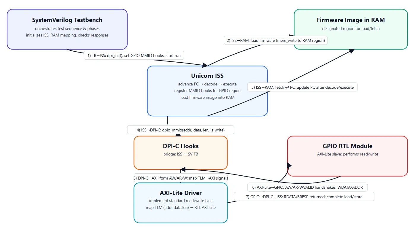
As shown in the architecture flow, the SystemVerilog testbench orchestrates the run while the Unicorn ISS loads firmware into RAM and executes it (advancing the PC, decoding/executing instructions, and trapping MMIO accesses). When firmware touches GPIO via MMIO, the ISS forwards the access parameters (addr, data, len) through DPI-C to the AXI-Lite driver.
The driver lowers these transaction-level fields into standard AXI-Lite handshakes and drives the GPIO RTL. When the transaction completes, the GPIO returns read data or a write response back along the same path to the ISS. This produces hardware-accurate MMIO behavior while keeping software execution fast.
Component responsibilities
1. Firmware Application
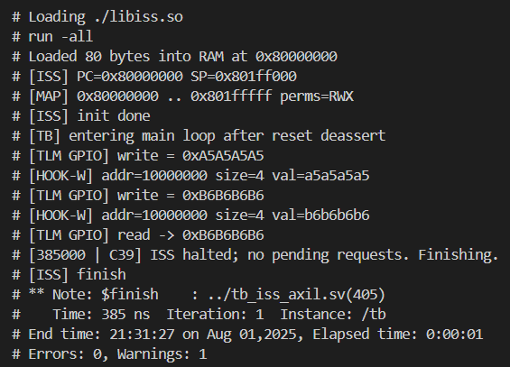
The sample firmware demonstrates the end-to-end path by performing simple MMIO operations:
- Write
0xA5A5A5A5and0xB6B6B6B6to a memory-mapped GPIO address - Read data back from the same memory-mapped GPIO address
- Exit using an
ebreakinstruction
2. RISC-V Unicorn ISS Layer
- Loads and executes firmware binaries (RISC-V 64-bit ELF)
- Provides hooks for instruction execution and MMIO access trapping
- Maintains its own simulated memory space, with GPIO address ranges marked as MMIO
3. DPI-C Bridge
- Implements the glue between C-based ISS code and the SystemVerilog testbench
- Uses
import "DPI-C"functions to pass transactions, memory reads/writes, and interrupt events - Encapsulates ISS-to-RTL exchanges so the ISS code is not tightly coupled to HDL code
4. SystemVerilog Testbench in QuestaSim
- Contains BFMs and signal-driving logic to emulate the memory system and peripherals
- Implements clock/reset generation, transaction routing, and signal assertions
- Captures simulation waveforms for debugging in QuestaSim GUI
5. Target Peripheral (RTL)
- A simple GPIO module connected through AXI-Lite
- Provides realistic read/write latency and responses
- Enables functional verification of firmware/hardware interaction through the ISS layer
This modular design means the ISS can be replaced with another RISC-V model, and the peripheral set can be extended, without overhauling the whole simulation infrastructure.
4. Simulation Workflow
The simulation uses a coordinated step-by-step exchange between the testbench, ISS, DPI-C bridge, and RTL peripheral:
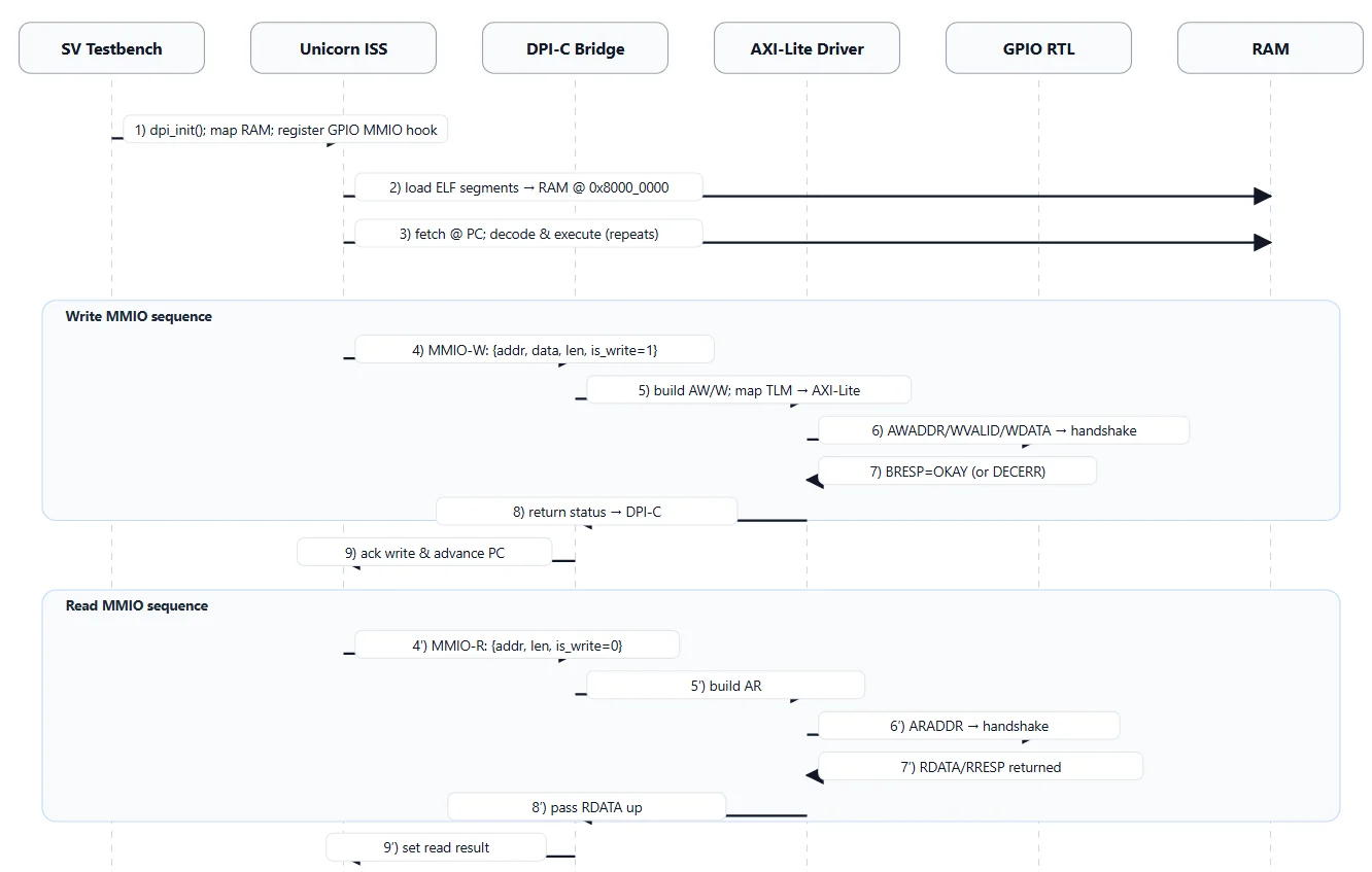
A typical run looks like this:
- The SystemVerilog testbench sets the pace (clock/reset and simulation timeline).
- The Unicorn ISS loads firmware into RAM and begins executing instructions.
- When firmware performs a GPIO MMIO access, the ISS pauses and packages the request (address, data, length).
- The DPI-C bridge forwards the request to the AXI-Lite driver in the testbench.
- The AXI-Lite driver performs the handshake with the GPIO RTL.
- The GPIO RTL returns read data or a write response.
- The response flows back through the same path to the ISS.
- The ISS resumes execution and continues until the next MMIO interaction or program exit.
This back-and-forth ensures memory-mapped I/O in the firmware is exercised against real hardware logic, making the simulation both realistic and precise.
The following screenshot shows the simulation result when running with QuestaSim:
Feel free to explore the repository, build the design, and tailor it to your needs. Detailed build and run instructions can live alongside the project with ready-to-use scripts.
5. Key Takeaways & Next Steps
This RISC-V-specific SW/HW co-simulation stack demonstrates that we can combine fast CPU emulation with cycle-accurate RTL simulation in a single DPI-based test environment with several practical benefits:
- Early firmware bring-up without waiting for FPGA or silicon
- Cycle-accurate hardware behavior for selected components
- Modular structure where ISS, DPI layer, and peripherals are independently replaceable
Potential next steps:
- Extend the ISS model to support privileged-mode features (for example, custom CSRs)
- Add more peripherals and DMA engines to broaden test coverage
- Implement timing models for more accurate cycle estimation
Closing Thoughts
A good co-simulation stack is not just a demo. It is an engineering multiplier. It lets firmware and hardware move in parallel, surfaces integration issues earlier, and gives teams a reusable validation path before FPGA bring-up or silicon.
If you want, I can also help turn this post into a more tutorial-style version next (with a concrete repo layout, DPI function signatures, and a minimal AXI-Lite transaction example).